On Wednesday, Mayor Alexander Pechtold ceremonially opened a new educational cleanroom at The Hague University of Applied Sciences on the Delft campus. The aim is to train more technical staff for the semiconductor industry.

The Beethoven Cleanroom will be used by the whole region: pupils from ROC Mondriaan and the Leiden Instrument Makers’ School, and students from The Haaagse Hogeschool, Inholland TU Delft. (Photo: @DeHaagseHogeschool)
“Just as a single wrong note can ruin an entire piece of music, a single stray particle of dust in the cleanroom can undermine a research project,” said Mayor Pechtold. To emphasise the pristine nature of the new cleanroom, two hosts briefly blow the stage clean with leaf blowers. Then the moment arrives: Mayor Pechtold and Elisabeth Minnemann, chair of the board of The Hague University of Applied Sciences, pull a lever, a large curtain falls, and the Beethoven cleanroom is officially opened.
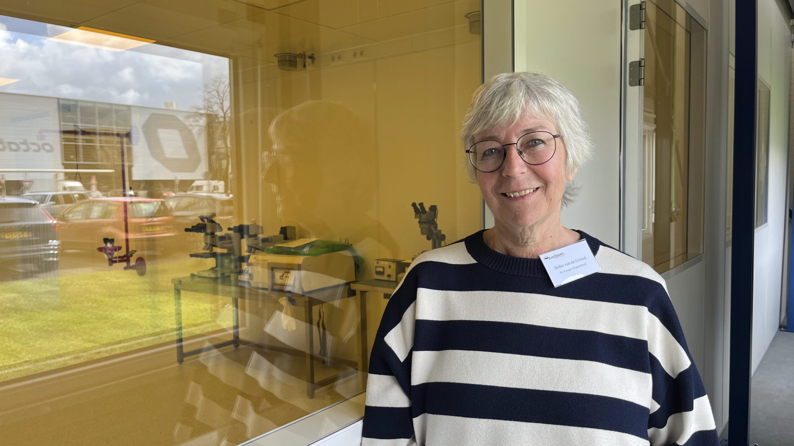
Nellie van de Griend, Faculty Director at The Hague University of Applied Sciences, is the programme manager for the Beethoven Programme and is responsible for overseeing the development of the cleanroom. She walks around with a big smile on her face, proud that they have managed to set up the cleanroom in just one year.
Project Beethoven
In 2024, the government decided to allocate €2.51 billion to ‘Project Beethoven’ to boost the Dutch semiconductor industry. €450 million is earmarked for training 38,000 additional technicians for the sector within six years: 14,800 from vocational education (mbo), 8,900 from higher professional education (hbo) and 14,500 with university degrees. The Beethoven Cleanroom will be used by the entire region: students from ROC Mondriaan and the Leiden Instrument Makers’ School, as well as students from The Hague University of Applied Sciences, Inholland University of Applied Sciences and Delft University of Technology.
Project Beethoven
If you imagine the cleanroom to be a white laboratory full of high-tech equipment you are in for a surprise. The space, measuring around 100 square metres, is still virtually empty. That is set to change in the coming months, explains Van de Griend during a brief tour. Entry is not permitted, to keep it as clean as possible. “This is where the wet benches will go – workstations for chemical processes, where gases and liquids are handled.” Apart from an eye wash and a safety shower, there isn’t much to see yet.
The yellow lighting in the rooms is striking; this protects the light-sensitive layers on the chips during the manufacturing process. The floor is conductive, to prevent static electricity. And the air is continuously filtered, so that it contains thousands of times fewer dust particles than normal air. “There will be eight workstations for actually making chips, to master techniques such as sputtering,” explains Van de Griend.
In addition to the fabrication area, where students learn step by step how a chip is made and thus also learn what sputtering is – the application of an ultra-thin layer onto a silicon wafer – on the other side of the lab is the assembly area, with workbenches equipped with apparatus. Here, the students get to work integrating chips into devices.
No machine without chips
Our demand for chips is growing, says Maarten Voncken of ASML. “Every device that runs on a battery or plugs into the mains contains chips. 90 per cent of those chips are manufactured on ASML equipment, worldwide. This market is enormous and continues to grow.” During the various talks held at the opening, the changing geopolitical landscape is discussed, and the importance of leading the way in the chip industry and collaboration is frequently mentioned. Not only within Europe, but also within educational institutions and the business community.
With the growing demand for Dutch chip technology, the need for qualified personnel is also increasing. Voncken: “At all levels: vocational, higher vocational and academic. The Beethoven programme is a huge help in this regard. We are training more people across a wide range of courses.”
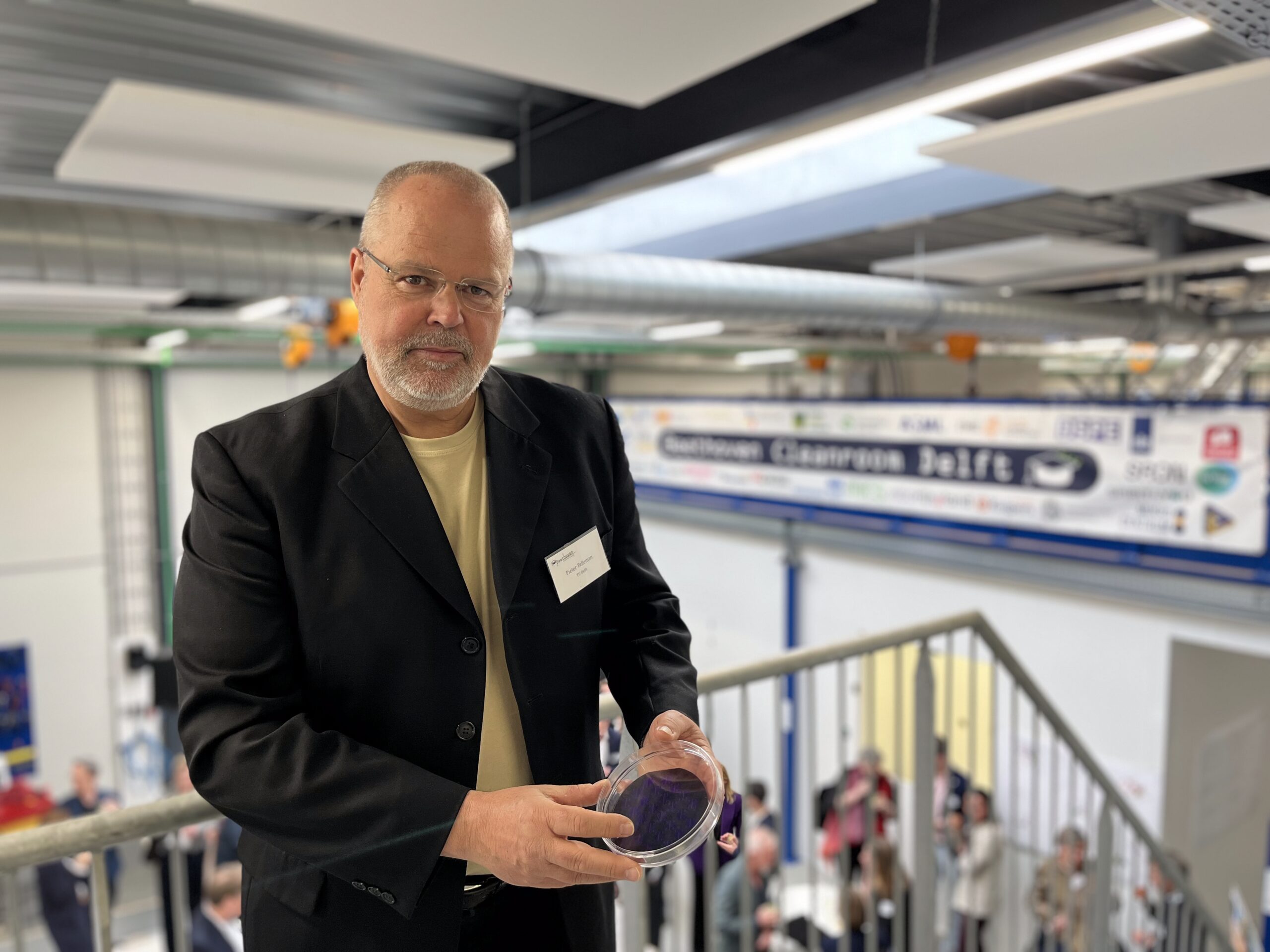
As Director of Cleanrooms at Delft University of Technology, Pieter Telleman is responsible for around 2,500 square metres of cleanrooms on the campus. Isn’t that enough to train new students? “In this teaching cleanroom, you’re allowed to make mistakes,” says Telleman. “There’s less scope for that in the top-tier facilities on campus where research is being carried out by various partners.” Telleman compares it to learning to drive. “You don’t get lessons in a Formula 1 car either. Here at Beethoven, we let people get used to working in the cleanroom step by step. There are instructors. And if you make a mistake, it doesn’t immediately have consequences for everyone around you.”
So how long will it be before the first students are actually trained here? It turns out, as early as the same day. Children from a primary school in Delft are coming to have a look. From November, the first TU students will be able to take a course.
Do you have a question or comment about this article?
E.Heinsman@tudelft.nl
Comments are closed.