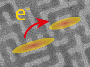
Researchers at TU Delft have found a way to connect nanocrystals using chemical bonds, allowing charge carriers to move through the network at ten times the speed of current networks, held together by organic molecules.
Networks made up of Lead Selenide (PbSe) nanocrystals, or ‘quantum dots’, are not a new discovery. What is interesting about the work done at TU Delft is the way in which they have connected the nanocrystals in networks. Professor Laurens Siebbels from the TU Delft department of Chemical Engineering of the Faculty of Applied Sciences lead the research for this paper. He explained to Delta how the team created their networks; “We connected these nanocrystals via atomic bonds and took away the organic molecules that are usually on the surface of these quantum dots.” By linking these PbSe Quantum Dots with direct chemical bonds instead of with organic molecules, as is usually done, the researchers from TU Delft created networks through which electrical charges can move more easily, increasing their speed.
With these chemically bonded networks, the speed of charges is allegedly increased ten-fold, making them potentially useful in a number of different areas. Professor Siebbels stated that he was “very pleased that we can achieve such a high mobility in efficient charge transport, and that we can easily generate charge carriers by irradiation with light.” This was in reference to the usefulness of this in solar cells particularly, as well as in field effect transistors and infrared light detectors.
The paper, published in September in the online Nature Communications journal, was worked on by researchers from TU Delft with collaboration from Utrecht University, the Foundation for Fundamental Research on Matter, and French CNRS.
Siebbels stated they currently have what is called a ‘square lattice’, and there are hopes the next step of the research will involve creating a honeycomb lattice, like in Graphene, to see how a different electronic structure may affect charge mobility. The researchers also aim to change Lead Selenide, the material used for this paper, to Cadmium Selenide, in order to see if the properties change further. Siebbels added that the ultimate hope is for this technology to be used in real devices, such as very efficient solar cells.


Comments are closed.