Professor Peter Steeneken is a man with a mission: making nanoscience applicable through nanoengineering.
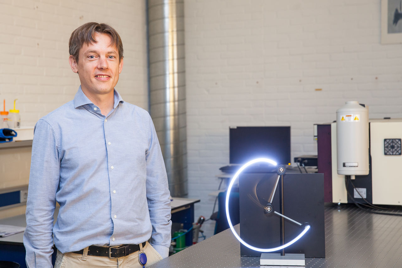
Professor Peter Steeneken in the lab (Photo: TU Delft)
There is plenty of room at the bottom, as Richard Feynman said. The problem has been to make use of it. Modern day technology has shown the potential of molecule-sized devices in the lab. But moving from the lab to mass-produced devices requires nanoengineering, says Professor Peter Steeneken (3mE and Kavli Institute of Applied Sciences). He will elaborate on his mission during his inaugural speech on Friday, 7 December 2018.
Sensors in smartphones
In the last few years, we have seen the first steps of graphene-topped nanostructures that might be used as sensors in smartphones. Other research has revealed that ballooning graphene could be used as a pressure sensor or a pixel.
Quality guarantees at nanoscale
Before these discoveries can be used in consumer devices, says Steeneken, we need to determine how to fabricate such tiny systems, and we need to develop quality guarantees at nanoscale. In short, we need to cultivate a new discipline called nanoengineering.
Much smaller, much more sensitive
And why do we need this? Because nanoscale sensors bring advantages beyond their small dimensions. Steeneken explains: “By using layers of nanometre thickness, we create pressure sensors that are much smaller and yet much more sensitive than their micrometre-sized counterparts. The thinness of the layers also allows us to create nanometre-sized holes, which can be used to sieve the air and selectively test for the presence of specific molecules.”
Inaugural speech
Steeneken will explain how the dynamics of electrostatically floating microscopic motors and switches help in making nanoscience applicable in his inaugural speech Dynamics in nanomechanics.
- Peter Steeneken, Dynamics in nanomechanics, Aula, 7 December 2018, 15:00.
- The inaugural speech will also be streamed through collegerama
Do you have a question or comment about this article?
j.w.wassink@tudelft.nl


Comments are closed.